|
Hey Nanotech Enthusiasts! This week, our special guests are two remarkable scientists from a team that pioneered a groundbreaking innovation in robotics and synthetic biology. Josh Bongard and Doug Blackiston are two of the brilliant minds behind xenobots. These biological machines made from cells have captured worldwide attention and created a new design paradigm for engineering with active materials. 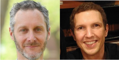 Welcome, Josh and Doug! Tell us about yourselves. What inspired you to get into STEM? Josh: I’m a computer scientist. Like many kids, I was fascinated by aliens, robots, and computers; I still am. So, I don’t think I ever “got into STEM”. I just kept learning about and, eventually, making, the things that had always interested me. Doug: I have an education background and previously taught in public middle and high schools. I also worked at Georgetown University in the Center For New Design in Learning and Scholarship (CNDLS), where I participated in a university-wide program aimed at understanding, and correcting, the high attrition rate among minority students within the biology major. Here in Boston, I've served as both a mentor and member for the Boston Scholars program, which pairs students from underrepresented populations in the Cambridge/Boston area with an adult mentor who guides them through all four years of high school. The BSP has a 100% college placement rate of all students coming through the program, compared to less than half for their non-BSP peers. While not specifically STEM learning, I'm very interested in increasing the participation of underrepresented groups in STEM fields. My view is that the approach should focus on the bottom up, growing scholars from local feeder populations and identifying where we are losing those students along the way. Your research on xenobots caused a lot of excitement. What are xenobots, and how do they differ from traditional robots? Josh: Traditional robots are made from metal and plastic: xenobots are, for now, made only from frog cells. Also: most robots are designed by human engineers. The xenobots are robots that are designed by an AI. Doug: Xenobots is a term used in the popular press very often, but I lean on the broader "biobot". Only recently have biological materials have been incorporated into the design of machines and robots, and I believe we were the first to use amphibian tissues (from the model system Xenopus laevis, hence the xeno-prefix). This can solve some problems facing traditional robotics--the material is biodegradable, programmable, and potentially self-regenerating. What inspired you to use biological materials in xenobots? Doug: Josh and Sam [Kriegman] had been working with virtual robots made out of programmable cubes, and had begun building those cubes out of silicon. I thought it could be possible to build their designs from living cells - and that traditional bioengineering programs might be looking at the wrong system. Xenopus is really the hero of the story - the model has been studied for ~80 years, tools exist to program collect and program their stem cells, all of their stem cells can survive in plain tap water, and it was known that some of their skin cells could self-propel in water due to micro-hairlike structures on their surface. They're also very robust, you can shape them, compress them, pull on them, and poke them and they tolerate the manipulations very well. What are the potential real-world applications of xenobots, and what are the primary challenges that need to be addressed in order to realize these applications? Josh: Like any new technology, it’s very hard to predict what its killer applications will be. For the xenobots, it’s like that, in the short term, they could be used for cleaning hazardous waste from ecologically sensitive environments. This is because xenobots are a green technology: they’re biocompatible and biodegradable. Doug: I agree with Josh here, there's a wide range of environmental applications as they are biodegradable. They are also non-reproducing, which removes the risk of them 'getting loose' and contaminating an ecosystem like and invasive species. For young people interested in pursuing a career in science and technology, what advice would you give ? Josh: Science and technology is really hard, but really rewarding. Most days, nothing works: code crashes, experiments fail, or other scientists and engineers don’t like your ideas. But, every once in a while, you see something in the lab, like xenobots, that no human has ever seen before. For me, this last reason is why I love what I do. Doug: People often think science and technology is somehow less expressive than arts related fields - I don't agree with this at all. If you have a curiosity and sense of wonder for the world around you, science can be incredibly fulfilling. I look in the microscope every week and see something no one has ever seen before, and solve problems that can make the world a better place. Suppose many years from now, xenobots were to become as advanced as the nanobots we see in science fiction. What jobs would you hire them to do for you? Josh: I don’t think xenobots of the future will be “them” and we will be “us”: instead, they’ll simply be part of our bodies. We’ll be able to, for example, send them out into the garden in the morning to grow a vegetable for dinner that tastes unlike any vegetable that’s ever existed, in the same way that we send texts out out in the morning and check responses on our phone later in the day. Doug: Building on Josh's analogy, I see parallels here with domestication. We've domesticated animals, plants, and microbes for human purposes, and I think we're only scraping the surface of how we can use biology to solve human problems. Like a traditional robot, I hope we'll be able to send biobots out into the environment where they can record their experiences, do work, and report back to the human at a later time. Thanks so much for taking the time to talk with us, and keep up the amazing research! Want to keep up to date on the latest happenings at DNP123? Subscribe to our newsletter.
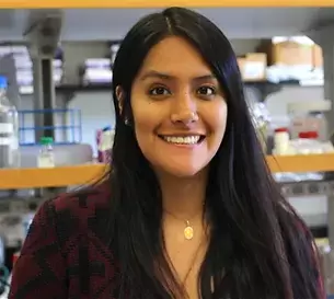
Tell us a bit about yourself. How did you get into science? My name is Paola Moreno-Roman. I was born and raised in Peru and moved to the US for graduate school, where I earned my PhD in Cellular and Molecular Biology. I've always been fascinated with studying life around me, and one of my earliest memories is spending hours observing a little caterpillar eat and move. However, it wasn't until I used a microscope to observe microorganisms that I fell completely in love with cellular biology. From that point on, I knew that I wanted to pursue a career in science and use my knowledge to make a difference in the world. Where did the idea for Foldscope come from? Foldscope was invented by Manu Prakash and Jim Cybulski. The invention occurred while Jim was a PhD student in Manu's laboratory at Stanford University. During visits to field stations, they repeatedly encountered bulky, broken microscopes or a lack of microscopes entirely. They realized the universal scale of this problem and the need for a low-cost, revolutionary solution. In the early days of the project, ideas for a low-cost microscope were sketched down on paper. These sketches ultimately led to the critical revelation that paper, a versatile and inexpensive material, could be folded into precise configurations to create a low-cost microscope. The project blossomed into the invention of Foldscope, a foldable microscope made mostly of paper that to this day still achieves the goal of being less than one U.S. dollar in parts. DNP123’s mission is making nanoscience affordable and easy enough for anyone. Foldscope’s highly affordable microscopes have been very inspirational for us in that regard. Tell us a bit about the impact Foldscope has had. What communities have benefited most from your work? Foldscope has had a significant impact in making microscopy accessible to communities around the world, particularly those with limited resources and access to traditional microscopes. Foldscope's affordability has enabled students, teachers, and scientists alike to explore and discover the microscopic world around them. Many different communities have benefited from Foldscope's work, including educators in developing countries, healthcare workers in rural areas, and citizen scientists. Foldscope has distributed thousands of microscopes to schools, research institutions, and NGOs worldwide, and their impact has been felt across a wide range of fields, including biology, ecology, and public health. We have distributed more than 1.8 million Foldscopes worldwide and reached 164+ countries. Foldscope’s website has an impressive list of publications. What are some of the most interesting projects you’ve seen done with a Foldscope? Since Foldscope was created, it has been involved in numerous impressive projects. Since I joined the company in July 2020, one of the most remarkable projects that I had the opportunity to be involved in was the partnership with Ector County Independent School District in Texas, USA. All 4th and 7th graders of that school district received a Foldscope. I had the pleasure of attending their summer camp in 2021, and witnessing firsthand the ways in which educators and students alike were able to adjust to the rapidly changing world and embrace innovative ways of learning. This project was a great success and truly highlighted the potential of Foldscope in science education. For more information about this project, readers can refer to this article: https://www.tepsa.org/resource/igniting-curiosity-and-discovery-through-a-new-lens-how-a-paper-microscope-created-new-opportunities-for-students-teachers-and-parents/. Where would you like Foldscope to be in 5-10 years? Foldscope is a tool that has the potential to become even more accessible and versatile for scientific research, education, and healthcare over the next 5-10 years. Foldscope could play a significant role in public health by detecting and monitoring diseases, particularly in low-resource settings, enabling diagnosis, screening, and monitoring. In science education, Foldscope has already been used to engage students in hands-on learning, and in the future, it could be integrated further into science curricula on a country-wide level to enhance students' scientific skills and literacy. Foldscope could also be used to monitor environmental quality, studying microorganisms and pollutants in various ecosystems, leading to informed environmental policies and promoting sustainability. Furthermore, Foldscope has the potential to empower citizens to participate in scientific research, enabling them to collect and analyze data in their communities, leading to a better understanding of local ecosystems and informing environmental and public health policies. In conclusion, Foldscope has the potential to be a powerful tool in a range of fields, democratizing science by making it more accessible and inclusive. Suppose some of our readers would like to get involved and purchase Foldscope kits. Where would they find them? If readers are interested in purchasing Foldscope kits, they can visit the official Foldscope website (https://www.foldscope.com/) to place an order. The website offers a variety of Foldscope kits, ranging from basic models to more advanced versions with additional features. Are there any new or upcoming Foldscope products you’d like our readers to learn about? Foldscope has recently launched online training workshops to help users acquire the basic skills needed to explore the microcosmos with their Foldscopes. Additionally, a new generation of Foldscope with multiple magnification lenses is in the works and will be released soon. If you had to hire a nanobot to do a job for you, what would the job be? If I had the opportunity to hire a nanobot for a job, I would choose to employ it to deliver iron directly to my red blood cells. As someone who suffered from anemia for several years, I know firsthand how long and slow the process of recovery can be with traditional iron supplements. By having nanobots deliver the iron directly to my red blood cells, I believe the recovery process could have been faster and more efficient. This could potentially revolutionize the treatment of anemia and other blood disorders, making them more manageable and efficient. Paola, thanks so much for taking the time to talk with us today! Keep us posted on your exciting work! Want to keep up to date on the latest happenings at DNP123? Subscribe to our newsletter.
Tell us a bit about yourself. What are you most passionate about? I am a science artist specialising in accurate biomedical animations of the molecular mechanisms that keep your cells alive. My animation presents the intricacies of human biology and disease as microscopic cinematic journeys inside your living cells to watch the chemistry of life in action. I construct animation by reviewing scientific literature on a topic, then combine and build with 3D molecular structures, dynamic simulation, speed measurement and many kinds of microscopy. Resonating most with large diverse audiences are animations from projects where I had plenty of time for research and data gathering, and consequently were as accurate as I could reasonably make them with lots of scientific detail. Whenever possible I try to let the science speak for itself and use real-time speeds to pace the shots and include as many layers of data as I can. I then go through a process of pruning out components that I feel are distracting or not supporting what the animation is trying to reveal. How did you get into animation, and why biomedical animations specifically? My science career began in a lab that specialised in filming the life and activity of microalgae, exquisitely beautiful single-celled organisms otherwise invisible to the naked eye. I was very fortunate to be mentored by one of the grand masters of microscopy Prof Jeremy Pickett-Heaps who taught me how to use various types of microscopes, how to keep cells alive and happy, and how to interpret what we could see. As a teen in the late 1980’s I was part of the first generation to grow up with a computer beginning with a monochrome TRS-80, then a Commodore 64, then my school’s Apple II with a dot-matrix printer. Ahh, good times. The most pivotal machine in my life was the Amiga 500 which I obtained around 1988, with its super advanced graphics and sound that was way ahead of its time. I wasted my summers on the Amiga playing video games and goofing around with computer graphics animation. My first cell biology animation was a mitotic cytoskeleton inside a dividing cell, created circa 1992 for an education video Jeremy’s lab produced on cell division and mitosis. The video was distributed on VHS cassette, so clearly I’ve been doing this for some time. Since 1995 I have been an artist in residence at WEHI, Australia’s flagship institute for medical research into diseases such as cancer, diabetes and malaria. What are some of the challenges of animating the microscopic world? All science at microscopic and molecular scale requires visual manipulation to make it watchable and meaningful for an audience. For the cellular dynamics, I strive for the look and feel of movements observed under time-lapse microscopy. The “Brownian motion” displayed in my molecular animation is a simple emulation of molecular dynamics simulations created with the various dynamics and game engines in 3D animation software, but with rates slowed down to make it watchable to a human audience. Beyond illustrating the science behind molecular machines, your animations display amazing artistry. The New Yorker called them "astonishingly beautiful." Tell us a little bit about the process of creating them. All of my inspiration comes from reading the scientific literature. I can't make stuff up that is better than the reality of how we work at the molecular and cellular scale. Most of my art sensibility was shaped by watching way too many science fiction and horror films from the 60's and 70's and being fascinated by the graphics of computer games and cinema. Sound design is 51% of what makes my animations come alive. It is subtle but powerful cue to the world you are looking at and makes the animations far more entertaining and engaging. Almost all of my animation soundscapes were created by my long-time friend and collaborator, Franc Tétaz, a Grammy-winning Australian sound designer and music producer. His sound design transforms my animation into a visceral experience which makes the audience lean in and engage. I know this might be like trying to pick a favorite child, but is there one animation you're particularly proud of? The animation that really opened my career was "DNA Replication" (2003), a 'real-time' visualisation of a double helix of DNA being copied, presenting the enzyme complex DNA replication machinery at work every time a cell divides. The animation was originally made for the Emmy winning documentary series “DNA” by Windfall Films, but then went onto the BAFTA-winning “DNA Interactive” DVD, and then proved surprisingly popular as Art exhibiting at many galleries around the world including MoMA, Guggenheim, V&A, Pompidou Centre and Melbourne ACMI. The most unexpected outcome is that the animation caught the eye of the Icelandic singer Björk, who contacted me out of the blue in 2009 wondering if I was interested in making a DNA Replication drum machine for her new album Biophillia. I ended up not only contributing to her DNA Replication drum machine, but also the Hollow animation music video for her Biophillia app album and concert stage shows. The COVID-19 pandemic revealed how important it can be for non-scientists to understand the microscopic world. Since our company mission is making nanoscience affordable and easy enough for anyone, what should companies like ours do to better communicate science? Show don’t tell. Avoid using the fancy language of science and never use acronyms. If you had to hire a nanobot to do a job for you, what would the job be? The nanobots I look forward to would be living ‘bio-bot’ ball of cells that can be switched onto the rejuvenation and renewal of my body, such as regrowing my skin as a 20-something. We could ask these bio-bots to grow new eyes for someone blind with glaucoma, repair the severed spine of a crash victim, or regrow missing limbs. With the current pace of discovery and research, I think this is feasible and will arrive in my lifetime. Drew, thanks so much for taking the time to talk with us today! If we ever do get bio-bots, we'll look forward to seeing your stunning animations of them! Want to keep up to date on the latest happenings at DNP123? Subscribe to our newsletter.
 We've got a special treat for our last Q&A of the year. DNP co-founder Aaron Santos had the opportunity to collaborate with the talented Selma Duhović of the Activation Energy podcast. We interviewed the Chemical Angel Network's Mark Vreeke about investing in deep tech in the chemistry space. Links below. Have a great holiday season!
• Spotify: bit.ly/3hJqmYX • Google: bit.ly/3vbpJus • Apple: bit.ly/3VcZUVv
Tell us a bit about yourself and your background. What are you most passionate about? I am a native Tulsan, and I started the company in the place where I was born. I'm passionate about other people and other entrepreneurs blooming where they are planted as well. As an entrepreneur and founder, I’m also passionate about giving people a good and respectful place to work. I didn’t realize before founding the company that people spend a lot of time in jobs in which this often isn’t the case. At Ten-Nine Tech, we focus on maintaining a respectful workplace and a place that rewards our team members for what they do. This allows them to express themselves and be the best at their jobs, and it has a lot to do with living a good and happy life overall. It's been surprising, even heartwarming, and important to me as a person, to feel as though I enable other people to achieve that in their workplace. You’re the founder and CEO of Ten-Nine Technologies. What are you hoping to accomplish through Ten-Nine Tech? I have two missions. The first is to develop and deliver the world's most powerful battery materials. We have to be a part of revolutionizing the electrification of the energy economy by making batteries work better. Batteries are a foundational tool for almost all other sustainable technologies. Reliable, renewable energy delivery depends on batteries, and batteries make an enormous difference in the life that we live every day. Most people think about battery life in terms of their cell phone, or an EV, but batteries are far more important in developing countries where they're running things – like light for a child to do their homework or an incubator to keep a baby alive. Batteries truly are one of those fundamental technologies that make a real-life difference to people around the world. And the second mission of Ten-Nine Tech is to build better batteries in a respectful workplace driven by our values of curiosity, generosity, and authenticity. To date, what’s been Ten-Nine Tech’s biggest success? Our biggest success to date is a scientific one - we were the first people to demonstrate fossil-fuel parity in a battery material. We developed a new material that is capable of delivering as much energy from the electrical reactions created in the battery material as can be garnered from combustion reactions in the burning of gasoline. That was an extremely significant demonstration, as no other batteries had come within a fraction of that sort of energy delivery, or energy density as we call it. Ever since then we've been working on how to practically use those energetic materials in batteries to make them perform better. Why was it important to found your own company rather than working at an existing company? And what are some of the benefits and disadvantages of working at a startup versus working at an established company? Let me tell you the story of how the company was started. I was approached by an angel investor while I was still working in academia who said, “you can't do what you need to do at a university,” and he was absolutely right! Universities do good things, but they're not set up to reach the marketplace or to make change in the marketplace. I think it’s important to recognize that. I've worked in academic, industry, and philanthropic settings, and I’ve learned that if you really want to change the world, you need to be in the marketplace. And the best way to do that is to found your own company. In addition, like many women I’ve found it very difficult to find a respectful and supportive work environment within existing companies. This is mainly because - for better or worse – existing companies (and universities, for that matter) were founded originally by men, and they were set up in ways that men found comfortable and appealing and that worked for them. It’s no wonder that women often find that existing workplaces don't work well for them. For me, it's been great to create a place in which the culture is respectful from the very beginning. It wasn't like we were trying to correct problems that other people set up. You're not trying to paint a door pink to get more women through it. You're just getting rid of the door and making a new entry. That’s one of the biggest advantages of founding your own company and building your workplace from scratch. What advice would you give to a student who thinks they might want to start their own company someday? I would encourage students who want to be founders to work at a startup. I certainly had an extraordinarily naive view of starting a business when I began in 2014. I've been able to overcome that deficit, but I would advise anyone to have a little more visibility on what a startup company looks like. One way to do that is to get an internship with a founder in your own community and bloom where you're planted. Don't think you have to go to Silicon Valley, or even work in the same type of company that you think you might start. But get a summer job with a start-up to see a glimpse of that world. Ask if you can shadow the founder - if you can sit down and talk to them about what the difficulties have been and how you should plan. Being on the inside somewhere and hearing from a founder who has walked that road is important. I’ve also found that once you start down that road, if you're a responsible person, you're very committed almost to the level of marriage or parenting. You are tied to that effort. It’s not something to take at all lightly but something to go into with seriousness and understanding. Learning from others will keep you from burning out or not being able to make and keep the commitments that you need to as a founder. In an interview with Startland News, you noted a commitment to creating opportunities for women at Ten-Nine. What are the biggest hurdles facing women in technology startups? The challenge for a woman founder is almost always that there are only women on one side of the table – and she’s the person asking for money or asking for a job, rather than the one handing out the money or hiring. When all of the managers or capital providers are men, that's never going to be a fair and equitable situation. Those men can be kind, they can see themselves as allies of women and advocates for women, but it is not an equivalent situation. The best way to overcome this huge hurdle is to get women on both sides of the table. When there are women on both sides of the table, whether that's a woman providing capital or a female founder interviewing for positions in a tech company, then opportunities for women will really change. The biggest outcome of not having women on the other side of the table is that women who found companies receive only two percent of the venture capital funding today. So, the biggest hurdle for women founders is simply getting capital. It means that you will have to pitch twice as many times as a man. You will have to answer twice as many questions, and it will take you twice as long. So right now, unfortunately, it's important for female founders to plan for that. I hope this will get better over time, but today, as a woman in technology, you must plan for what we know to be true. One of the things I found fascinating about your bio was your breadth of curiosity including everything from children’s playgrounds to atomic gardening. Tell us a bit about your non-professional interests. That's a lovely way to state it – “breadth of curiosity!” You know, of course, that curiosity is one of the company’s three core values. I find that because I'm a curious person, I want to create a company culture that's like myself in that way. Curiosity is obviously a key component of my personality and it's something we look for in the people that come to work for Ten-Nine Tech. I ask potential employees if they have a passionate second interest, and, as you noted, I have multiple passionate second interests. I often tell people that I have a hungry mind that works best when it is engaging with knowledge rather deeply. For years before I started a company I was blogging about children's playgrounds and the history of gardens. While I was still at the university, I was able to maintain all those interests and write about all those interests. I do love to write, which is something that has served me very well. As a founder, there's a little bit of additional advice to people wanting to start a company - you need to be a good writer. When you are early stage, you have to write your own press releases, your own ad copy, your own grants, your own reports, and your own board materials. Being a good communicator goes along ways towards giving you that additional boost toward success. Now about my non-professional interests - I love the creation of a space for people to inhabit. I love gardens. I love landscapes whether they are atomic gardens or children's playgrounds. I love to understand how humans deal with nature and utilize nature to create and inhabit space. The last question is something we like to ask all our interviewees. If you had to hire a nanobot to do a job for you, what would the job be? Because I like to delve deeply into things, I always have a far greater reading load than I can manage - from scientific papers related to batteries and nanotechnology to garden and history books. I've always said that my superpower would be to be able to touch a book and consume the knowledge in it immediately. As a lover of knowledge, I would hire a nanobot to read for me. Paige, thank you so much for taking the time to talk with us today! Good luck making our electric future a reality! Want to keep up to date on the latest happenings at DNP123? Subscribe to our newsletter.
Tell us a bit about yourself. What are you most passionate about? Hmm! I'm probably most passionate about enabling helpers and joy. This comes from a perspective of mortality and pessimism: I've got probably under 50 years of being able to do stuff, and there are lots of problems locally and globally that I feel powerless to fix. One tangible facet of being an educator, however, is empowering people to solve problems and teach, too, and that makes me hopeful some big problems get solved. It's also easy to forget that hilarious things are ubiquitous, and there's joy to be found in finding them, in discovering things, in helping others in spite of things not being perfect. I think it's very important to experience joy, especially in ostensibly "professional" settings, in order to do sustained work on hard problems. One of your research goals is to “leverage thermodynamics for societal good”. What are some examples of this? The sorts of things my team is trying to do include projects like discovering chemicals that are good ingredients for inexpensive solar panels, and understanding how the polymers used to make aircraft composites can be used to make stronger, lighter, more efficient aircraft at lower cost. In both cases, the properties of the materials, whether they're strong enough for airplanes or good at converting light into electricity, depends on how the molecules making the materials are arranged. The laws of thermodynamics govern how those molecules arrange themselves when we mix them together, and so we work hard to understand how to exploit those laws to work for us when making new materials. But the ultimate goal of the new materials we aim to invent is for them to be easy to make without harming the planet, reliable, and useful in helping people live safely and sustainably. Experimentalists typically run experiments in labs to test how materials work. Theoreticians do calculations to predict how materials work. How would you describe how computational scientists work? Is it more experimental or theoretical? There's wide variance in whether computational scientists lean more experimental and theoretical, and it's possible to do lots of both! Most of the time on my team, the work we do is more experimental: We set up an experiment using a computer, perform the experiment, and have a look at the results in the same way that someone using a fume hood or glove box might. We can do more experiments in a shorter amount of time, often, but when we're not working with theory to develop new kinds of experiments, we're mostly performing experiments using computers as the apparatus. High-performance computing using graphics cards dramatically expanded they types of simulations scientists can do. With the rise of machine learning and the potential coming of quantum computing, what do you predict materials research will look like in 10 to 20 years? There's potential, and I am hopeful, that many arduous, important, but uncreative tasks will have been replaced with fast computations. For example, the creation and evaluation of the rules by which atoms interact in simulations is something we set up by hand right now, is very fiddly, and there's no fundamental reason we couldn't train a machine to do this for us. It looks like there's great potential for quantum computers to assist with the prediction of the electronic structure of molecules, which would put a whole set of techniques out of business. But I don't have a good sense for, theoretically, whether some fundamental problems in materials science are as "easy" as playing go for teachable machines. In 2015, I thought computers beating top professional players at go was 10 years away, and it happened in 2016. The successes of AlphaFold are super inspiring and I'm hopeful to see something similar be usable in predicting the structure of, say, polymer materials, for example. In summary, I think that in the next two decades it should be a lot easier to to predict the structure of materials from their ingredients, and because of this, those that can predict properties from structures or those that can figure out how to synthesize those structures will be even more sought after. The description in your Twitter account lists bikes and Go as interests in addition to science. How important is it to have interests outside science? Do these interests ever overlap with your research? Without some balance it's possible to ruin anything. Like, eating one slice of pizza is great, but having to eat 500 in one sitting is terrible. The research I do gives me time away from riding bikes, which gives me time away from playing go. I love doing all of those things, but if could only do one of them I expect I'd have under 20 years of attention before I burned out at it. So they're different enough that I can get a break from one when doing another, but there's a ton of overlap between them! Fixing bikes and debugging code are identical processes on different machines. Finding the best move on a go board and finding the energy-minimizing structure of a polymer are essentially equivalent mathematically. Winning a bike race and go tournament both require training, strategy, and split-second decision-making. In all three cases you can be a professional, and my experiences interacting with experts in each domain inform how I think about teaching, mentoring, competition, and supporting communities in the others. How would students describe what it’s like to work on your research team? You should ask the students on our team! I hope they'd say it's a fun, supportive, interesting place to work and learn. If you had to give a high school student interested in STEM careers advice, what would you say? There are a ton of different careers that scientists, engineers, and mathematicians can do, and many of them you'll find interesting and fulfilling. Find them and do them, we need you! It's also a sad truth that many of the systems and practices in STEM education make students feel excluded from their classes, departments, and universities. Universities aren't immune to sexism or racism, and there's a lot of work to be done to make STEM opportunities more equitable. If you feel like sexism or racism hasn't mattered to your education so far, I'd invite you to use that privilege to help effect change. Reading broadly around the history of science and education is just as important as reading broadly about the the topics that got you interested in STEM careers. If you had to hire a nanobot to do a job for you, what would the job be? Delete emails before they reach my inbox? Haha, no, maybe turn things off that are wasting energy? OK. So, nanobot, huh? I'm interpreting "nano" as some things whose size is less than say 500nm, and "bot" to mean things that are programmable. So this is like 10x to 100x smaller than a red blood cell, so it'd be great to have some in my arteries disposing of plaque, allowing me to eat as much jamon iberico I want. But if we can program trillions of them to build more of each other, who can place the molecules in the right places for custom materials, then we're done, right? This is a tall order, though, because I know how hard it is to program things correctly, and how fiddly things are at nanometer scales, so I worry that half-reasoned attempts to do this end up causing more havoc than good. Eric, thanks so much for taking time to talk with us! I look forward to reading your future publications! Want to keep up to date on the latest happenings at DNP123? Subscribe to our newsletter.
DNP123 CEO Aaron Santos had the pleasure of speaking about nanotech entrepreneurship with NNCO Director Lisa Friedersdorf on the Nano Entrepreneurship Network podcast. Check it out here: Want to keep up to date on the latest happenings at DNP123? Subscribe to our newsletter.
Tell us about yourself. What are you most passionate about? I lead a nanomedicine and extracellular vesicle research program in the School of Chemical Engineering and the Australian Institute for Bioengineering and Nanotechnology at the University of Queensland in Australia. I am actively involved in community outreach and scientific education, and as a TED speaker I strive to bring science to a wider audience. I am equally passionate about three things: 1) developing new therapeutics and diagnostics that have the potential to help patients with life-threatening diseases, 2) developing the next generation of leaders in biomedical research, and 3) increasing diversity in science What first interested you in nanoscience? Conventional medicines are angstrom sized. By developing medicines on the larger nanoscale we have opportunities to combine several components to develop new medicines with multiple functions that result in better outcomes for patients and less side effects. According to your faculty page, your research centers on nanomedicine with the goal of developing innovative approaches that bring the next generation of treatments and diagnostics directly to the clinic. What are some promising approaches you’re researching now? My research program is engineering the body’s own transportation system (biological nanoparticles) to precisely deliver medicine for improved therapeutic effects with less side effects. What are some of the hardest challenges of moving technology from the lab to the clinic? Funding and predicting clinical results in simpler models. Your science career has taken you all over the world. You did your undergrad in Finland at the University of Helsinki, your PhD at University of Chinese Academy of Sciences, you had a faculty position at Mayo Clinic, and you’re now an Associate Professor at the University of Queensland in Australia, just to name a few. Are there a lot of cultural differences in how different countries conduct scientific research? What are some of the benefits you’ve found from doing research in such diverse places? Scientific culture is global. Every institute provides a unique learning experience. I have been lucky to work in different places and to absorb and implement diverse research practices along my journey. According to your Wikipedia page, your mother is artist. Did you do any artistic work growing up, and if so, did it help your science career at all? Arts and science should be more closely linked. Both are creative processes. Many education and outreach activities implement art in various forms (e.g., dancing) to illustrate complex scientific topics. I had the pleasure of working with you on the Cancer Nanovaccine Game through Houston Methodist. STEM outreach, particularly outreach aimed at underrepresented minorities in science, seems to be a passion of yours. What do you think is the best way to get young people hooked on science? I think it is important to reach underrepresented minorities in biomedical research early on in order to make sure that everyone is exposed to science as a potential career option. One way of doing this is through interactive and educational games that are broadly accessible. I am really excited about the NanoVaccine game that we developed because it introduces the concept of vaccines, nanomedicine, and the immune system in a fun and easily understandable way. Joy, thank you so much for taking time to talk with us. It was a pleasure working with you on the NanoVaccine game. Good luck in your research endeavors! Want to keep up to date on the latest happenings at DNP123? Subscribe to our newsletter.
Tell us a bit about yourself and your career. What are you passionate about? I am a true STEM interdisciplinary at heart, both in my academic and professional career. I obtained my Bachelor of Science Degree in Biochemistry and Molecular Biology with a cognate in Biotechnology from Michigan State University; a Master's Degree in Chemistry from Fisk University; and a Doctoral Degree in Environmental Sciences/Engineering Physics from Wright State University. I’ve worked as a Materials Engineer for the Air Force Research Laboratory, Process Development Engineer in industry, and served as an Academic Dean, Department Chair, and Associate Professor at various colleges and universities throughout Southern California. I am truly passionate about bringing exposure of the STEM fields, particularly science and engineering, to underrepresented groups locally and globally. How did you first get interested in nanoscience? I first became interested in science when I was a child. My parents bought me my first telescope and microscope when I was just 12 years old. I would go outside with my father in the evenings and collect anything and everything to be able to bring it back inside my home and dissect. I was always fascinated with how things behaved inside and out! Your Google Scholar page features a pretty diverse research background. You’ve had publications featuring everything from graphene to DNA-based electronic devices. How would you describe your research interests to a young person? That's a great question. I would describe my research as being innovative and still ongoing. My research involves one of the most abundant elements found on Earth: carbon! Carbon has so many cool and neat properties that this element alone is used in so many everyday devices. For example, a cell phone, a tablet, and a laptop computer to name a few. I'd show how using such an abundant element on Earth such as carbon has many benefits especially when paired with DNA based materials. It is low cost, and most importantly, environmentally friendly. You’ve worked in both academia and industry. What would you say are the differences between the two? There are so many differences between the two. I strongly believe if you are a hands-on type of person and like "growth" both mentally and career-wise, industry is the way to go. It provides better opportunities for networking and not to be siloed into doing your own thing. There is also room for research collaborations and more opportunities in general in industry than academia. Academia doesn’t offer as much room for growth or professional development, and you run the risk of being siloed. Lastly, academia has a much lower salary.  Dr. Williams works at BioTeam, a life sciences IT consulting company. Tell us a bit about BioTeam. What drew you to your new position there? What kind of work are you doing? BioTeam is a life sciences IT consulting company passionate about accelerating scientific discovery by closing the gap between what scientists want to do with data—and what they can do. Our mission is to accelerate science. Working at the intersection of science, data and technology since 2002, BioTeam has the interdisciplinary capabilities to apply strategies, advanced technologies, and IT services that solve the most challenging research, technical, and operational problems. Skilled at translating scientific needs into powerful scientific data ecosystems, we take pride in our ability to partner with a broad range of leaders in life sciences research, from biotech startups to the largest global pharmaceutical companies, from federal government agencies to academic research institutions. At BioTeam we are scientists, data scientists, and technologists who are experts at translating scientific needs into a solution that works for an organization. I love this because we are here to help scientists achieve their goals. I’m really excited to be part of a team that is changing the world through scientific discovery. What advice would you give to a freshman high school student inspired by your work? What’s the best thing they can do to prepare for a career in nano or other sciences? Be curious! Curiosity has led to the most innovative technologies we use today. If you do not have curiosity, you will not be creative in your own right. Own your work and keep striving for greatness. This will carry you throughout your academic and professional career. Finally, accept failure or loss. Success requires failure. You will learn to become a better problem solver and provide many solutions to a problem. Last Question: If you had to hire a nanobot to do a job for you, what job would you hire it to do? I would definitely hire a nanobot to have my breakfast and morning coffee ready, sitting at my desk before I begin work. I definitely need the energy boost in the mornings, sometimes in preparation for back-to-back meetings and working on high-level projects. Adrienne, thank you so much for taking time to share your work with us, and good luck helping scientists achieve their goals with BioTeam! Want to keep up to date on the latest happenings at DNP123? Subscribe to our newsletter.
Tell us a bit about yourself. What inspired you toward a career in nanoscience? Since a kid, I have always been passionate about design and engineering. When my friends were drawing Batman cartoons, I was drawing modifications to the Batmobile. After graduate school in Chemical Biology studying pathways involved in cancer, I wanted to move into more engineering and design. I wanted to solve problems, not just ask questions. As I was trained in biochemistry and specifically DNA structure and function, nanotechnology was an obvious application of my expertise to an engineering problem. This past semester, you did undergraduate research with your organic chemistry lab students. Why is undergraduate research important? What challenges arise when conducting research with students? Undergraduate research is about gaining appreciation for the material you are learning. Simply, putting it use. The most difficult part of undergraduate research is gaining independence. Independence takes time to develop and is a difficult journey of learning how to ask the right questions and plan ahead. When working with students, I am constantly trying to find a balance between guidance and independence. Especially early in their journey to independence, students need close guidance. The difficult part is finding the right time to step back and let them start to work independently. Again, this is a long process and the earlier students can start on the path toward independent scientist, the more they can accomplish. What questions were you hoping to answer this semester? My goal with research in the undergraduate classes is to provide appreciation for the science the students are learning. The current students have been embroiled in several years of the COVID pandemic disrupting their life, and I wanted to ensure that the students are connecting the science they are learning to their daily lives. In the lab section of the class, we worked on a genetic test for HIV mutations. Similarly to the coronavirus, HIV can mutate. A predominant mutation, G48V allows HIV to function in the presence of commonly used protease inhibitors therapies. In the lab section of the class, I showed the students how to coat DNA onto surfaces like glass to make a common bioassay for identifying G48V mutant HIV. You yourself were once an undergraduate research student at Simpson. If you had to go back in time, what career advice would you give 18-year-old Derek? Network more. Solving real problems requires a wide range of skill sets and viewpoints. I have found the most success in my career collaborating. Is there any additional advice you'd give students looking to do research today? Get involved in research as early as possible. Research provides an application to what you are learning and will certainly guide you to finding a true passion, a place to focus your attention in the vast world of science. Discovering your passion project requires many misadventures along the way to find the magical combination of a problem that you care about that matches your skill set, interests, and available resources. Last Question: If you had to hire a nanobot to do a job for you, what job would you hire it to do? I live in suburbia, which roughly translates into the "land of beautiful landscaping". The harder I work on my making my yard look good, the worse it gets. I need some nanobots to help - maximize soil nutrients, minimize invasive weed species. Derek, thank you so much for taking time to catch us up on your work! Want to keep up to date on the latest happenings at DNP123? Subscribe to our newsletter.
|
 RSS Feed
Home |
About |
Services |
Menu |
Contact |
Copyright © 2018